SOLIDWORKS PCB —powered by Altium— is a new software solution focused on integrating electrical and mechanical design. SOLIDWORKS PCB enables the productivity you need to design Printed Circuit Boards (PCBs) quickly along with unique collaboration between electrical and 3D mechanical design teams. To efficiently manage your PCB design workflow, it is important to be thorough and detailed in the initial set up of your designs.
You can ensure a successful PCB layout by correctly setting up your board design environment. Once the environment is set up, begin your component placement and routing. In SOLIDWORKS PCB, there are both global settings, which can set your preferences across many designs, and local or project-specific settings.
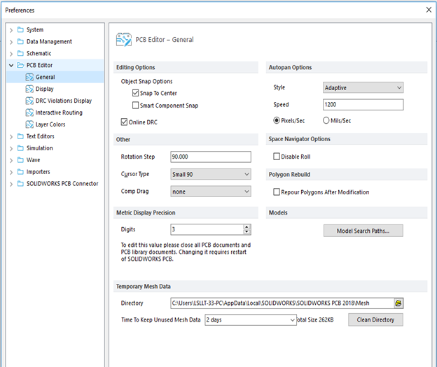
Global Setting Options
Global settings include options such as cursor settings, display options, error markings, default routing behavior, etc. You can access these through File – System Preferences – PCB Editor. It is even possible to export and share these global settings with other users to standardize across your organization!
Configuring your design environment for your specific project needs within each unique PCB project is even more critical, and a bit more involved. Let’s take a look at the various options you will want to take advantage of to complete your board layout smoothly.
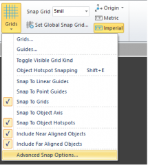
First, you will want to make sure to set your origin, select your units, and set up your grid spacing. Your origin can be easily changed and moved around throughout the design process if needed, but it is good practice, to begin with, it in the lower left of your design space.

When selecting your units and setting up your grids, keep in mind the units and grid settings that were used when you developed your PCB footprints. These settings will ensure that your components can be easily aligned and that your traces will connect to your component pads without any dangling lines or off-grid connections.
Next, you will want to define your board stack up using the Layer Stack Manager.
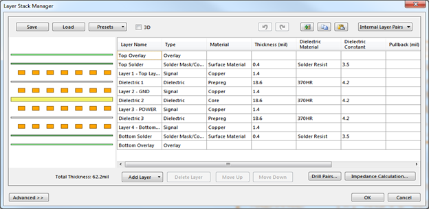
There are default options built-in for a standard 2, 4, 6, 8, 10, 12, 14, and 16-layer board, but you can also define your own stack up. If you have a specific board house that you use and have complete stack-up details defined from them, you can create your own template and save it so that it is always readily available. Be sure that this information is complete and accurate as it will be generated within your output files and used for manufacturing. Even more importantly, this is the data that will be used to collaborate your board design with SOLIDWORKS MCAD and in 3D Visualization.
Customize Your Settings
After you’ve gotten your layer stack up defined, you’ll want to customize the color/view setting for each layer.
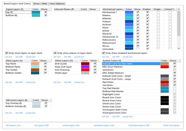
Color coding for each specific layer can be extremely helpful throughout the layout process. That way traces, pads, polygons, keep-outs, etc. are easily distinguishable and you won’t waste time trying to decipher what is what throughout your layout.
The last major piece that you’ll want to set up before you begin your board layout is your design rules.
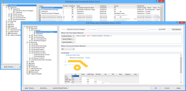
Being as thorough and complete as possible while setting up your design rules will simplify the routing process. Setting up width constraints in terms of minimum width, preferred, and maximum width allows you to seamlessly toggle through width options while interactively routing your board. You can even set up these rules down to the specific net. The same goes for vias. Remember to pay careful attention to your priorities, as this will also affect how the rules are followed within your design.
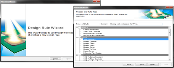
For precise, customized rules, make use of the Rule Wizard to generate specialized rules according to numerous selectable constraints automatically. Setting up your rules as accurately as possible will also make your auto-router more valuable.
To get more updates on SOLIDWORKS Follow Us on LinkedIn: Click Here
For more details Like Us on Facebook: Click Here
For videos SUBSCRIBE to our channel: Click Here
For more information: Click Here
